Search

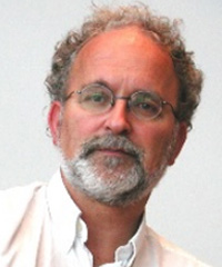
Prof. Fred Roozeboom, University of Twente, The Netherlands
K2-2: 11:30-12:15, Oct. 23, 2024, Wednesday
Title: Atomic Layer Processing: Its Evolution, Diverse Applications, and Future Prospects
Abstract:
In sub-10 nm scaling and fabrication of 3D architectures, especially the techniques of ALD and ALE have manifested to cost-effectively bridge the >10-years incubation time needed to bring EUV technology from prototype to commercial use. More importantly, these unique techniques can be used to create advanced devices by using dedicated isotropic (thermal and radical-enhanced) and anisotropic (directional and ion-enhanced) processing. Here, energetic species (radicals and/or ions in a plasma) are used in one or two steps, with the ions yielding anisotropic profiles (used in FinFET logic and 3D NAND memory), and neutrals and radicals yielding isotropic profiles used to deposit or etch the features in single-digit-nm device architectures containing horizontal nanowires, nanosheets and ‘forksheets’ in GAA-FETs, and complementary FETs.
Biography:
Prof. Dr. Fred Roozeboom received his MSc in chemistry (cum laude) from Utrecht University, Netherlands, in 1976, and his PhD in chemical engineering in 1980 at Twente University (Enschede, Netherlands) in heterogeneous catalysis.From 1980-1983 he worked on zeolite catalysis with Exxon/Mobil R&D Labs in Baton Rouge, USA (1980-1982) and with Exxon Chemicals in Rotterdam (1983).In 1983 he joined Philips Research (since 2006: NXP) in Eindhoven, Netherlands, where his early work encompassed MOCVD of III-V semiconductor lasers (1983-1988), IC metallization (1988-1990) and on bulk ferrite and thin-film soft-magnetic materials for magnetic recording (1990-1996). In 1996 he worked on MBE of ultrathin magnetic and ‘switchable mirror’ hydride multilayers.From 1997 to 2009 he led a team working on passive and heterogeneous integration, in particular on viahole technology and 3D integration for application in System-in-Package products and on high-value passives in silicon for application in wireless communication (RF decoupling), power management, and digital signal processing. Two technology transfers on 3D passive integration (PICS® wireless technology) to Philips' /NXP Semiconductor plants in Caen-France (now Murata Integrated Passive Solutions S.A.) and ASMC’s foundry in Shanghai-China resulted in over 400 M$ accumulated sales in the 2003-2008 period. For part of this work he received the Bronze Award of the ‘NXP Invention of the Year 2007’ and became an NXP Research Fellow in 2007. Another important application of the high-capacitance trench capacitor technology has been developed into miniaturized pacemaker production by Medtronic, USA, now used for minimum-invasive implantation.In 2009 he left NXP, and joined TNO-Holst Centre in Eindhoven, Netherlands, until 2021, as a senior technical advisor working in a team specializing in spatial Atomic Layer Deposition and related processing, e.g. Atomic Layer Etching and Cleaning (incl. EUV optics cleaning).In 2011, the spatial processing team at TNO received the 2nd EARTO Innovation Award.In 2014 he was elected Fellow of the Electrochemical Society.In 2023 he was elected as the recipient of the ECS Gordon E. Moore Medal, and also as Fellow of the American Vacuum Society, and winner of a 2023 Gerard & Anton High-Tech Star Award.


 loading......